-

深圳市伟格兴电子科技有限公司
主营:集成电路销售,二三极管销售

深圳市伟格兴电子科技有限公司
主营:集成电路销售,二三极管销售 18
18

TERMINOLOGY
Integral Nonlinearity (INL)
INL is the maximum deviation from a straight line passing
through the endpoints of the ADC transfer function. For the
AD7476A/AD7477A/AD7478A, the endpoints of the transfer
function are zero scale (1 LSB below the first code transition),
and full scale (1 LSB above the last code transition).
Differential Nonlinearity (DNL)
DNL is the difference between the measured and the ideal
1 LSB change between any two adjacent codes in the ADC.
Offset Error
This is the deviation of the first code transition (00 . . . 000) to
(00 . . . 001) from the ideal, that is, AGND + 1 LSB.
Gain Error
This is the deviation of the last code transition (111 . . . 110) to
(111 . . . 111) from the ideal, that is, VREF – 1 LSB after the offset
error has been adjusted out.
Track-and-Hold Acquisition Time
The track-and-hold amplifier returns to track mode at the end
of a conversion. The track-and-hold acquisition time is the time
required for the output of the track-and-hold amplifier to reach
its final value, within 0.5 LSB, after the end of conversion. See
the Serial Interface section for more details.
Signal-to-Noise-and-Distortion-Ratio (SINAD)
This is the measured ratio of **-to-noise-and-distortion at
the output of the ADC. The ** is the rms amplitude of the
fundamental. Noise is the sum of all nonfundamental **s up
to half the sampling frequency (fS/2), excluding dc. The ratio is
dependent on the number of quantization levels in the digitization
process; the more levels, the smaller the quantization noise.
The theoretical **-to-noise-and-distortion ratio for an ideal
N-bit converter with a sine wave input is given by **-tonoise-and-distortion
= (6.02 N + 1.76) dB. Thus, it is 74 dB for
a 12-bit converter, 62 dB for a 10-bit converter, and 50 dB for an
8-bit converter.
Total Unadjusted Error (TUE)
This is a comprehensive specification that includes the gain,
linearity, and offset errors.
Total Harmonic Distortion (THD)
Total harmonic distortion is the ratio of the rms sum of
harmonics to the fundamental. It is defined as
1
2
6
2
5
2
4
2
3
2
2
V
V V V V V
THD
+ + + +
(dB) = 20log
where V1 is the rms amplitude of the fundamental, and V2, V3,
V4, V5, and V6 are the rms amplitudes of the second through the
sixth harmonics.
Peak Harmonic or Spurious Noise (SFDR)
Peak harmonic or spurious noise is defined as the ratio of the rms
value of the next largest component in the ADC output spectrum
(up to fS/2 and excluding dc) to the rms value of the fundamental.
Normally, the value of this specification is determined by the largest
harmonic in the spectrum. For ADCs where the harmonics are
buried in the noise floor, it is a noise peak.
Intermodulation Distortion (IMD)
With inputs consisting of sine waves at two frequencies, fa and
fb, any active device with nonlinearities create distortion
products at sum and difference frequencies of mfa, nfb, where
m and n = 0, 1, 2, 3, and so on. Intermodulation distortion
terms are those for which neither m nor n are equal to zero. For
example, the second-order terms include (fa + fb) and (fa – fb),
and the third-order terms include (2fa + fb), (2fa – fb), (fa + 2fb),
and (fa – 2fb).
The AD7476A/AD7477A/AD7478A are tested using the CCIF
standard where two input frequencies are used (see fa and fb in
the Specifications section). In this case, the second-order terms
are usually distanced in frequency from the original sine waves,
while the third-order terms are usually at a frequency close to the
input frequencies. As a result, the second- and third-order terms
are specified separately. The calculation of the intermodulation
distortion is per the THD specification, where it is the ratio of
the rms sum of the individual distortion products to the rms
amplitude of the sum of the fundamentals expressed in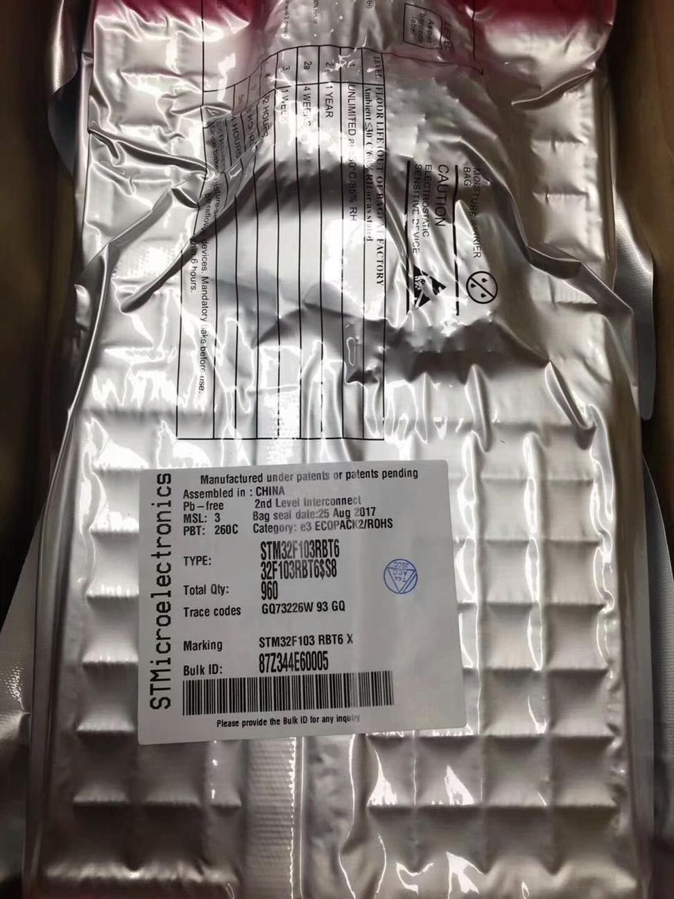
ADP5065的充电参数——比如快速充电电流、充电终端电
流和充电终端电压——均可通过I2
C接口编程设置。这种可
编程性使ADP5065能用于多种类型的锂离子电池,同时还
可作为完整的电池充电和测试控制器使用。
电池放电控制和电子负载(E-Load)电路
图2中虚线框内的电子负载(E-load)电路提供了可编程恒流
负载,采用AD8601精密CMOS运算放大器、4个1 W、1%功
率电阻,以及2个功率SIR464 MOSFET。
E-load电流目前由AD8601同相输入端上的控制电压精确控
制。控制电压(MCU板上的V_DAC)范围为0 V至1 V,产生
的负载电流为0 A至2 A。锂离子电池的典型放电终端电压
为3.0 V。此E-load允许的输出电压小值为:
基板提供输入/输出板和MCU板之间的连接。用户可以通
过不同的I2
C DEV_ID访问特定输入/输出板上的ADP5065和
ADG715。图7中的逻辑采用ADuCM360的3位通用输入/输
出(GPIO)将SCLK信号路由至适当的输入/输出板。可以增
加更多通道;但是,更多的通道需要更高的ADC采样速
率、更大的MCU RAM尺寸、更快的放电电压刷新速率,以
及更高的上级处理器通信带宽。
电池通道数可以通过增加更多EVAL-CN0352-EB1Z系统扩
展,它们共享一个RS485总线,连接PC。这种情况下,每
一个模块都必须具有范围为1至255的ID。ID0保留。
CN-0352评估软件扫描所有ID并记录各可用ID的ID和通道
编号。注意,RS485总线的波特率将会是使用这种方式时
通道扩展的限制因素。
电路性能测量
系统噪声在电池连接器上测得,测量时将电池电压检测引
脚V+和V−短路(如图3所示),并测量ADC输出码在2000点
采样间隔期间的峰峰值变化。对电流通道执行类似的测
量。对于温度通道而言,连接10 kΩ固定电阻,而不是热敏
电阻。其结果分别显示在图8、图9和图10中。
假定一个N通道系统的采样和保持时间分别为TS
和TH,则
必须满足下列条件:
因此,更多的通道需要更长的保持时间,而漏电流导致电
压下降更大。对于CN-0352系统而言,N = 8,TS
= 1 ms,
TH = 7 ms,电压下降可以忽略。
热管理
大多数锂离子电池无法在低于0°C或**60°C的温度下充
电。快速充电和放电只能在10°C到45°C范围内进行。
除了安全问题,锂离子电池的性能也可能随着温度而大幅
改变。因此,应精确测量电池温度,确保测试结果的可重
复性,同时也为了确保安全性。
使用10 kΩ热敏电阻监控电池温度,该热敏电阻通过双线式
连接温度连接器模块。待测电池通常位于电路板附近,因
此热敏电阻引线电阻可以忽略。
输入/输出板上还有另一个10 kΩ电阻,它连接ADP5065的
THR引脚,如图2所示。